 Lebanese Ministry of Information
Scientists say the technology could make devices faster, less dense, and consume less energy
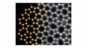
The world’s smallest piece of technology – only two atoms thick – has been created by researchers to store electric information.
Current state-of-the-art devices consist of tiny crystals that contain approximately one million atoms, one hundred atoms square. In a computer, these devices switch between two binary states (one and zero, yes and no, up and down) to encode and process information.
Scientists say they can now make that process even more efficient. Reducing the size of the technology down to only two atoms enables the electrons to move through the layer at a greater speed. The difference is somewhat similar to a large button that requires a great amount of force to push, compared to a smaller, thinner one that requires less force.
These are also the benefits the researchers are touting for practical devices that use this technology: they would be faster, less dense, and consume less energy.
The study, published in the journal Science, uses a one atom-thick layer of boron and another of nitrogen arranged in a repeated hexagonal structure.
“In the lab, we were able to artificially stack the layers in a parallel configuration with no rotation, which hypothetically places atoms of the same kind in perfect overlap despite the strong repulsive force between them (resulting from their identical charges).
“In actual fact, however, the crystal prefers to slide one layer slightly in relation to the other, so that only half of each layer’s atoms are in perfect overlap, and those that do overlap are of opposite charges—while all others are located above or below an empty space—the centre of the hexagon.
“In this artificial stacking configuration the layers are quite distinct from one another. For example, if in the top layer only the boron atoms overlap, in the bottom layer it’s the other way around.”
When the electrical field is applied in the opposite direction, the system slides to switch orientation, and remains stable even when that field is shut down. These innovations are not unique to boron and nitrogen, and using this interlayer sliding as a way to control electronics is “promising”, Dr Shalom said.
In addition to computer devices, the scientists expect that this technology will contribute to the development of other detectors, energy storage and conversion, and gadgets that interact with light.
The Independent